https://twitter.com/x/status/1738454665359138996
Despite the lack of access to advanced chip production equipment due to U.S. sanctions, China-based SMIC remains committed to developing post-7nm fabrication processes, such as 5nm and 3nm, according to a report from Nikkei.
Having developed its 2nd-gen 7nm-class process technology, which is good enough for smartphone processors, the report claims that SMIC has now dedicated a research and development team to working on 5nm- and 3nm-class process technologies, citing two sources with knowledge of the matter. The team is led by co-CEO Liang Mong-Song, who used to work at TSMC and Samsung and is considered one of the best semiconductor scientists and executives in the industry.
"There is not any smarter scientist or engineer than that guy," Dick Thurston, former chief legal counsel at TSMC, told EE Times earlier this year. "He is really one of the more brilliant minds I have seen in semiconductors."
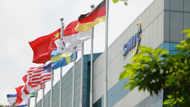
SMIC has come a long way from being a small foundry in China; today it is the industry's No. 5 contract maker of chips. Amid growing tensions between the U.S. and China, the company was listed on the U.S. Department of Commerce's Entity List and lost access to leading-edge wafer fab tools, severely slowing its progress and adoption of new process technologies.
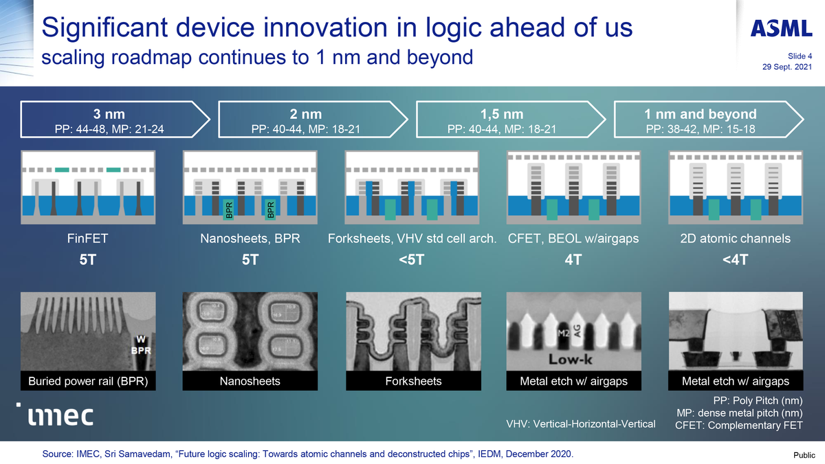
As a result, SMIC couldn't get extreme ultraviolet (EUV) lithography tools from ASML, so the company's second-gen 7nm-class node relies solely on deep ultraviolet (DUV) lithography. This isn't an incredible feat, given that TSMC's N7P process node also doesn't use EUV. For now, ASML's Twinscan NXT:2000i lithography machines are the best tools SMIC has, and they can etch production resolutions as fine as 38nm. This level of precision is adequate for printing 38nm metal pitches using double patterning, which is suitable for 7nm-class nodes. At 5nm, metal pitches shrink to 30 – 32nm, and at 3nm, they drop to 21 – 24nm, according to ASML and IMEC. Therefore, EUV becomes crucial for these nodes.
But using lithography tools with ultra-fine resolution (13nm for Low-NA EUV) is not the only path to achieving ultra-small feature sizes — multi-patterning is an option, but this is a complicated process that lengthens cycle times, can affect yields, wears fab equipment, and certainly increases costs. However, without EUV tools, SMIC simply has no choice but to use triple, quadruple, or even quintuple patterning to achieve lower resolutions.
Thurston believes that under co-CEO Liang Mong-Song, SMIC can produce (if it is not already producing) 5nm chips in large quantities without using EUV tools. We have heard mentions of 5nm-class process technology from SMIC several times already, so we would consider information about this potential node as 'there is no smoke without fire.' However, this is the first time we have heard about SMIC's possible ability to design a DUV-only 3nm-class fabrication process from a largely reliable source.
Here is another video . Despite being few months old , it tells a lot about how Chinese companies are smart enough to not getting bothered/halted by US Sanctions
Post and article are few months old but speak about China's growing strength in tech war
https://twitter.com/x/status/1710131927926313299
Blacklisted Chinese chipmaker SMIC is working on 3nm process technology despite US sanctions that limit access to advanced tools: Report
Despite the lack of access to advanced chip production equipment due to U.S. sanctions, China-based SMIC remains committed to developing post-7nm fabrication processes, such as 5nm and 3nm, according to a report from Nikkei.
Having developed its 2nd-gen 7nm-class process technology, which is good enough for smartphone processors, the report claims that SMIC has now dedicated a research and development team to working on 5nm- and 3nm-class process technologies, citing two sources with knowledge of the matter. The team is led by co-CEO Liang Mong-Song, who used to work at TSMC and Samsung and is considered one of the best semiconductor scientists and executives in the industry.
"There is not any smarter scientist or engineer than that guy," Dick Thurston, former chief legal counsel at TSMC, told EE Times earlier this year. "He is really one of the more brilliant minds I have seen in semiconductors."
SMIC has come a long way from being a small foundry in China; today it is the industry's No. 5 contract maker of chips. Amid growing tensions between the U.S. and China, the company was listed on the U.S. Department of Commerce's Entity List and lost access to leading-edge wafer fab tools, severely slowing its progress and adoption of new process technologies.
As a result, SMIC couldn't get extreme ultraviolet (EUV) lithography tools from ASML, so the company's second-gen 7nm-class node relies solely on deep ultraviolet (DUV) lithography. This isn't an incredible feat, given that TSMC's N7P process node also doesn't use EUV. For now, ASML's Twinscan NXT:2000i lithography machines are the best tools SMIC has, and they can etch production resolutions as fine as 38nm. This level of precision is adequate for printing 38nm metal pitches using double patterning, which is suitable for 7nm-class nodes. At 5nm, metal pitches shrink to 30 – 32nm, and at 3nm, they drop to 21 – 24nm, according to ASML and IMEC. Therefore, EUV becomes crucial for these nodes.
But using lithography tools with ultra-fine resolution (13nm for Low-NA EUV) is not the only path to achieving ultra-small feature sizes — multi-patterning is an option, but this is a complicated process that lengthens cycle times, can affect yields, wears fab equipment, and certainly increases costs. However, without EUV tools, SMIC simply has no choice but to use triple, quadruple, or even quintuple patterning to achieve lower resolutions.
Thurston believes that under co-CEO Liang Mong-Song, SMIC can produce (if it is not already producing) 5nm chips in large quantities without using EUV tools. We have heard mentions of 5nm-class process technology from SMIC several times already, so we would consider information about this potential node as 'there is no smoke without fire.' However, this is the first time we have heard about SMIC's possible ability to design a DUV-only 3nm-class fabrication process from a largely reliable source.
Here is another video . Despite being few months old , it tells a lot about how Chinese companies are smart enough to not getting bothered/halted by US Sanctions
Post and article are few months old but speak about China's growing strength in tech war
https://twitter.com/x/status/1710131927926313299